


CIRCUIT DIAGRAM DESCRIPTION
POWER SUPPLY:
The present chapter introduces the operation of power supply circuits built using filters, rectifiers, and then voltage regulators. Starting with an ac voltage, a steady dc voltage is obtained by rectifying the ac voltage, then filtering to a dc level, and finally, regulating to obtain a desired fixed dc voltage. The regulation is usually obtained from an IC voltage regulator unit, which takes a dc voltage and provides a somewhat lower dc voltage, which remains the same even if the input dc voltage varies, or the output load connected to the dc voltage changes.
A block diagram containing the parts of a typical power supply and the voltage at various points in the unit is shown in fig. The ac voltage, typically 120V rms, is connected to a transformer, which steps that ac voltage down to the level for the desired dc output. A diode rectifier then provides a full-wave rectified voltage that is initially filtered by a simple capacitor filter to produce a dc voltage. This resulting dc voltage usually has some ripple or ac voltage variation. A regulator circuit can use this dc input to provide a dc voltage that not only has much less ripple voltage but also remains the same dc value even if the input dc voltage varies somewhat, or the load connected to the output dc voltage changes. This voltage regulation is usually obtained using one of a number of popular voltage regulator IC units. voltage changes. This voltage regulation is usually obtained using one of a number of popular voltage regulator IC units.
THREE-TERMINAL VOLTAGE REGULATORS:
Fig shows the basic connection of a three-terminal voltage regulator IC to a load. The fixed voltage regulator has an unregulated dc input voltage, Vi, applied to one input terminal, a regulated output dc voltage, Vo, from a second terminal, with the third terminal connected to ground. For a selected regulator, IC device specifications list a voltage range over which the input voltage can vary to maintain a regulated output voltage over a range of load current. The specifications also list the amount of output voltage change resulting from a change in load current (load regulation) or in input voltage (line regulation).

The series 78 regulators provide fixed regulated voltages from 5 to 24 V. Figure 19.26 shows how one such IC, a 7812, is connected to provide voltage regulation with output from this unit of +12V dc. An unregulated input voltage Vi is filtered by capacitor C1 and connected to the IC’s IN terminal. The IC’s OUT terminal provides a regulated +12V which is filtered by capacitor C2 (mostly for any high-frequency noise). The third IC terminal is connected to ground (GND). While the input voltage may vary over some permissible voltage range, and the output load may vary over some acceptable range, the output voltage remains constant within specified voltage variation limits. These limitations are spelled out in the manufacturer’s specification sheets. A table of positive voltage regulated ICs is provided in table.
FINGERPRINT RECOGNITION MODULE

In this project we are using a fingerprint sensor named R303A for sensing the fingerprints of the voters. It is interfaced with the port3 of the MC.
Specification
Interface: UART(TTL logical level) & USB 1.0
Dimension: 56*20*21.5mm
Image Capture Surface 18*23mm
Verification Speed < 1 second
Scanning Speed < 0.5 second
Character file size:256 bytes
Template size: 512 bytes
Storage capacity: 120/375/880
Security level: 5(1,2,3,4,5(highest))
False Acceptance Rate (FAR) < 0.001%
False Rejection Rate (FRR) < 0.1%
Resolution
Voltage 3.6-6.0V DC via USB port
Working current: Typical 100mA , Peak 150mA,Matching Method 1:N
Operating Environment Temperature: -15 to 45 centigrade
Operation Principle
Fingerprint processing includes two parts: fingerprint enrollment and fingerprint matching (the matching can be 1:1 or 1:N).When enrolling, user needs to enter the finger two times. The system will process the two time finger images, generate a template of the finger based on processing results and store the template. When matching, user enters the finger through optical sensor and system will generate a template of the finger and compare it with templates of the finger library. For 1:1 matching, system will compare the live finger with specific template designated in the Module; for 1:N matching, or searching, system will search the whole finger library for the matching finger. In both circumstances, system will return the matching result, success or failure.
Hardware connection
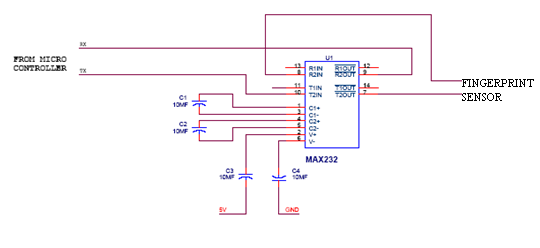
Via serial interface, the Module may communicate with MCU of 3.3V or 5V power: TD (pin 2 of P1) connects with RXD (receiving pin of MCU), RD (pin 3 of P1) connects with TXD (transferring pin of MCU). Should the upper computer (PC) be in RS-232 mode, please add level converting circuit, like MAX232, between the Module and MC.
Serial communication protocol
The mode is semi duplex asynchronism serial communication. And the default baud rate is 57600bps.User may set the baud rate in 9600~115200bps。
Transferring frame format is 10 bit: the low-level starting bit, 8-bit data with the LSB first, and an ending bit. There is no check bit.
Reset time
At power on, it takes about 500ms for initialization. During this period, the Module can’t accept commands for upper computer.
RS232 COMMUNICATIONS
In telecommunications, RS-232 is a standard for serial binary data interconnection between a DTE (Data terminal equipment) and a DCE (Data Circuit-terminating Equipment). It is commonly used in computer serial ports.
Scope of the Standard:
The Electronic Industries Alliance (EIA) standard RS-232-C [3] as of 1969 defines:
Electrical signal characteristics such as voltage levels, signaling rate, timing and slew-rate of signals, voltage withstand level, short-circuit behavior, maximum stray capacitance and cable length
Interface mechanical characteristics, pluggable connectors and pin identification
Functions of each circuit in the interface connector
Standard subsets of interface circuits for selected telecom applications
Details of character format and transmission bit rate are controlled by the serial port hardware, often a single integrated circuit called a UART that converts data from parallel to serial form. A typical serial port includes specialized driver and receiver integrated circuits to convert between internal logic levels and RS-232 compatible signal levels.
Circuit working Description:
In this circuit the MAX 232 IC used as level logic converter. The MAX232 is a dual driver/receiver that includes a capacitive voltage generator to supply EIA 232 voltage levels from a single 5v supply. Each receiver converts EIA-232 to 5v TTL/CMOS levels. Each driver converts TLL/CMOS input levels into EIA-232.


In this circuit the microcontroller transmitter pin is connected in the MAX232 T2IN pin which converts input 5v TTL/CMOS level to RS232 level. Then T2OUT pin is connected to reviver pin of 9 pin D type serial connector which is directly connected to FPM.
In FPM the transmitting data is given to R2IN of MAX232 through transmitting pin of 9 pin D type connector which converts the RS232 level to 5v TTL/CMOS level. The R2OUT pin is connected to receiver pin of the microcontroller. Likewise the data is transmitted and received between the microcontroller and FPM or other device vice versa.
MICROCONTROLLER UNIT
Here the popular microcontroller AT89C51 from ATMEL GROUP is used as the CPU of the system. This is a popular 8 bit microcontroller in the world. They are available in wide variety in pin outs, memory capacity and have lots of integrated peripherals like ADCs, SERIAL and EEPROM.
AT89C51 is the 40 pins, 8 bit Microcontroller manufactured by Atmel group. It is the flash type reprogrammable memory. Advantage of this flash memory is we can erase the program with in few minutes. It has 4kb on chip ROM and 128 bytes internal RAM and 32 I/O pin as arranged as port 0 to port 3 each has 8 bit bin .Port 0 contain 8 data line(D0-D7) as well as low order address line(AO-A7).
Port 2 contain higher order address line (A8-A15). Port 3 contains special purpose register such as serial input receiver register SBUF, interrupt INT0,INT1 and timers T0 , T1 many of the pins have multi functions which can be used as general purpose I/O pins (or) Special purpose function can be decided by the programmer itself.
Specification:
• 4K Bytes of In-System Reprogrammable Flash Memory
Endurance: 1,000 Write/Erase Cycles
• Fully Static Operation: 0 Hz to 24 MHz
• Three-Level Program Memory Lock
• 128 x 8-Bit Internal RAM
• 32 Programmable I/O Lines
• Two 16-Bit Timer/Counters
• Six Interrupt Sources
• Programmable Serial Channel
• Low Power Idle and Power Down Modes
The AT89C51 is a low-power, high-performance CMOS 8-bit microcomputer with 4K bytes of Flash Programmable and Erasable Read Only Memory (PEROM). The device is manufactured using Atmel is high density nonvolatile memory technology and is compatible with the industry standard MCS-51™ instruction set and pin out.
The on-chip Flash allows the program memory to be reprogrammed in-system or by a conventional nonvolatile memory programmer. By combining a versatile 8-bit CPU with Flash on a monolithic chip, the Atmel AT89C51 is a powerful microcomputer which provides a highly flexible and cost effective solution to many embedded control applications.
The major Features of 8-bit Micro controller ATMEL 89C51: CMOS
8 Bit CPU optimized for control applications
Extensive Boolean processing (Single - bit Logic ) Capabilities.
On - Chip Flash Program Memory On - Chip Data RAM
Bi-directional and Individually Addressable I/O Lines
Multiple 16-Bit Timer/Counters
Full Duplex UART
Multiple Source / Vector / Priority Interrupt Structure
On - Chip Oscillator and Clock circuitry.
On - Chip EEPROM
SPI Serial Bus Interface
Watch Dog Timer
ALARM CIRCUIT

Buzzer:
A buzzer or beeper is a signalling device, usually electronic, typically used in automobiles, household appliances such as a microwave oven, or game shows. It most commonly consists of a number of switches or sensors connected to a control unit that determines if and which button was pushed or a preset time has lapsed, and usually illuminates a light on the appropriate button or control panel, and sounds a warning in the form of a continuous or intermittent buzzing or beeping sound. Initially this device was based on an electromechanical system which was identical to an electric bell without the metal gong (which makes the ringing noise).
Often these units were anchored to a wall or ceiling and used the ceiling or wall as a sounding board. Another implementation with some AC-connected devices was to implement a circuit to make the AC current into a noise loud enough to drive a loudspeaker and hook this circuit up to a cheap 8-ohm speaker. Nowadays, it is more popular to use a ceramic-based piezoelectric sounder like a Sonalert which makes a high-pitched tone. Usually these were hooked up to "driver" circuits which varied the pitch of the sound or pulsed the sound on and off.
Circuit description:
The circuit is designed to control the buzzer. The buzzer ON and OFF is controlled by the pair of switching transistors (BC 547). The buzzer is connected in the Q2 transistor collector terminal.
When high pulse signal is given to base of the Q1 transistors, the transistor is conducting and close the collector and emitter terminal so zero signals is given to base of the Q2 transistor. Hence Q2 transistor and buzzer is turned OFF state.
When low pulse is given to base of transistor Q1 transistor, the transistor is turned OFF. Now 12v is given to base of Q2 transistor so the transistor is conducting and buzzer is energized and produces the sound signal.
Table 2.
Voltage signal from microcontroller | Transistor Q1 | Transistor Q2 | Buzzer |
1 | On | Off | off |
0 | Off | On | on |
KEYPAD
A numeric keypad, or numpad for short, is the small, palm-sized, seventeen key section of a computer keyboard, usually on the very far right. The numeric keypad features digits 0 to 9, addition (+), subtraction (-), multiplication (*) and division (/) symbols, a decimal point (.) and Num Lock and Enter keys. Laptop keyboards often do not have a numpad, but may provide numpad input by holding a modifier key (typically lapelled "Fn") and operating keys on the standard keyboard.
Particularly large laptops (typically those with a 17 inch screen or larger) may have space for a real numpad, and many companies sell separate numpads which connect to the host laptop by a USB connection.Numeric keypads usually operate in two modes: when Num Lock is off, keys 8, 6, 2, 4 act like an arrow keys and 7, 9, 3, 1 act like Home, PgUp, PgDn and End; when Num Lock is on, digits keys produce corresponding digits. These, however, differ from the numeric keys at the top of the keyboard in that, when combined with the Alt key on a PC, they are used to enter characters which may not be otherwise available: for example, Alt-0169 produces the copyright symbol. These are referred to as Alt codes.
On Apple Computer Macintosh computers, which lack a Num Lock key, the numeric keypad always produces only numbers. The num lock key is replaced by the clear key.

LED CIRCUIT

In electronics, the basic LED circuit is an electrical circuit used to power a light emitting diode (LED). It consist of up to four components connected in series: a voltage source, a current limiting resistor, a LED, and optionally a switch to open and close the circuit. The switch may be replaced with another component or circuit to form a continuity tester. Two diodes may be placed in parallel in the circuit, but connected anode to cathode: the second diode may be used to protect the LED against reverse bias, which can damage the LED, or it may be another LED which is illuminated when the polarity of the voltage source is reversed.
The LED s used will have a forward voltage specified at the intended operating current. When the voltage source Ohm’s law is used to calculate the resistor that is used to attain the correct current The resistor value is computed by subtracting the forward bias voltage from the supply voltage, and then dividing by the desired operating current.
16X2 LCD DISPLAY
A 16x2 LCD display is interfaced with the MCU in order to provide instructions to the voter. LCD stands for Liquid Crystal Display. The most commonly used LCDs found in the market today are 1 Line, 2 Line or 4 Line LCDs which have only 1 controller and support at most of 80characters.
Here the LCD display is interfaced with the MC through the port0 pins. Each instruction given to the MC will display on the LCD screen. This will provide complete instructions to the voter.
EEPROM
EEPROM (also written E2PROM and pronounced "e-e-prom," "double-e prom," "e-squared," or simply "e-prom") stands for Electrically Erasable Programmable Read-Only Memory and is a type of non volatile memory used in computers and other electronic devices to store small amounts of data that must be saved when power is removed.
EEPROM is interfaced with the MCU that can act as a database to store the thumb impressions of the voter. Here the EEPROM is interfaced with the port1 pins of the microcontroller to store the fingerprints of each voter’s. When the fingerprint sensor reads a finger the microcontroller store the data in the form of binary levels in the EEPROM.